


JasonDoiy
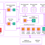
Samsung (OTCPK:SSNLF) received an order from Tokyo-based AI firm Preferred Networks to make chips for AI applications using the South Korean company’s 2-nanometer foundry process and advanced 2.5D packaging technology Interposer-Cube S (I-Cube S).
Samsung noted that the chips will be manufactured using a chip architecture called Gate-All-Around, or GAA, and several chips will be integrated in one package to boost inter-connection speed and reduce package size.
“This order is pivotal as it validates Samsung’s 2nm GAA process technology and Advanced Package technology as an ideal solution for next-generation AI accelerators,” said Taejoong Song, Corporate VP and the head of Foundry Business Development Team at Samsung.
Samsung added that since starting mass production of 3nm process node applying the GAA architecture, it has strengthened its GAA technology leadership by winning orders for the 2nm process with more upgrades in performance and power efficiency.
By using Samsung’s foundry and advanced packaging products, Preferred Networks aims to develop powerful AI accelerators to meet the growing demand for computing power driven by generative AI.